
Intoduction to the Prototyping Module for RC2014
The Prototyping Module for the RC2014 allows you to easily create projects to interface with your Z80 Projects that use the RC2014 bus. The Prototyping module does a lot of the work for you. It will decode the port address, and provide you with useful pins such as I/O Enable, Read, and Write pins. You can purchase this module from the Tindie Website. The purpose of this post is to simply get you started with the prototyping module.
Basically, you just set the jumpers to the port address that you want your I/O to respond to. It’s important to realize this port number is in Hexadecimal. Keep in mind that if you use the example address of 0x50-0x53, this will be 80 to 83 in decimal. It’s easy to forget to convert the address if you are using the I/O Addresses in BASIC.
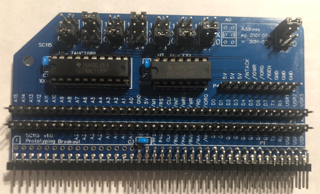
IC’s and Settings on the Prototyping Module for RC2014
This module has two IC’s. The 74HCT688 decodes the address you select from the jumpers. If you need your project to use a wider range of addresses, simply set the jumpers to the center position for the bits you don’t want to decode. For example, if you set all the jumpers to 1 or 0, then you will only have 2 addresses available. If you set the last jumper to X (center position), the 75HCT688 will set the I/O enable pin high for 4 port addresses. Likewise, if you set the last 2 jumpers to the center position, then the board will respond on 8 port addresses. It works a lot like the subnet mask in Ethernet Addressing.
The M1 Setting is for Machine cycle 1. When the first machine cycle is in progress, the M1 pin is low. When the first machine cycle is complete, M1 will go high again. In this case, we’ll set the M1 jumper to 1, which means we will enable our I/O when the first machine cycle is complete. At this point, the Z80 refreshes the address bus.
The 74HCT32 provides you with useful pins such as Interrupt Acknowledge, I/O Enable, I/O Read, and I/O Write. You will find the schematic for this module at this link (Page #5)
Wiring the Outputs
In the example I show here, I’m just turning on 8 LED’s. We’ll keep this simple. The connections will be easy since I’m not accounting for any switches, or other devices.
On the breadboard, we need to have 8 LED’s with the current limited by ~470 Ohm resistors. I’ll also set up a 74HCT374 on the breadboard. This is not only a buffer, but also will hold the outputs on. In other words, we don’t want the outputs to only be on for one clock cycle. We want them to stay on until we write a different value to the LED’s.
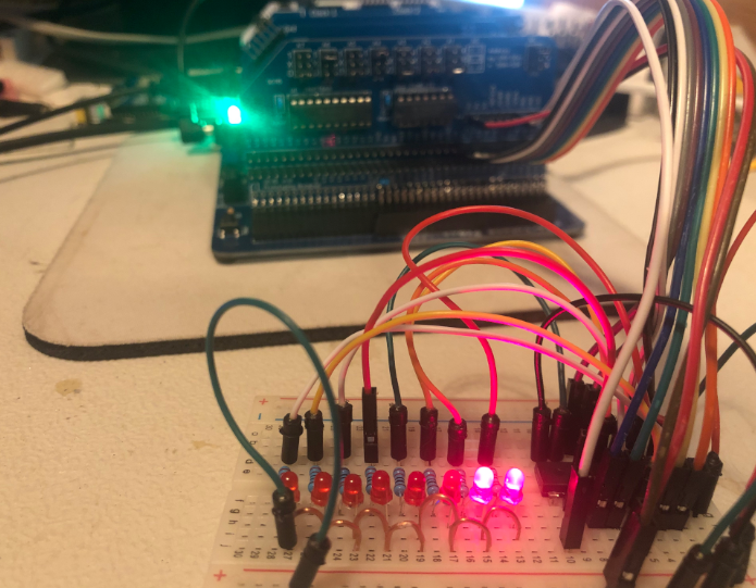
You will find the pinout of the 74HCT374 here. Basically, you just connect power up to the IC. After that, you will connect D0 on the Prototype Board to D0 on the 74HCT347. Likewise, D1 to D1, and so on. I connected the Output Enable pin (#1) to ground.
Since I am not using any inputs, I didn’t even worry about the IO Read and Write pins. I just connected the IO Enable pin to the clock pin. As far as the LED’s themselves, you will tie them to Q0 to Q7. Don’t forget that you need a current limiting resistor for each of the outputs. The cathodes of the LED’s will go to ground.
After powering up my system, I just went straight into BASIC, and issued the command OUT 80,255. That turned on all of the LED’s. Remember that 50 hex is 80 decimal.
Expanding Your Project
Once you get the LED’s to work, then you understand how the board works. You are ready to expand your project. I would recommend taking a look at the Digital I/O Board Schematic to understand how to incorporate switches with lights. To expand your project, you will likely need to do some more decoding to further narrow down the port numbers to specific functions on your breadboard. Additionally, you will need logic to determine whether the current operation is a read or write. Be careful not to write your switches to the data bus when another devices is writing to the bus at the same time.
For more information on vintage computers, visit the Vintage Computer category page!
— Ricky Bryce