
Introduction to Wiring any Logic using only NAND Gates
I’ve heard people say before that you can hard wire any logic using only NAND Gates. I started researching this a little bit, and purchased some NAND gate IC’s (74HC00). In this post, we’ll see how we would wire AND, OR, and NOT logic using ONLY NAND gates.
The NAND gate simply inverts the output signal from an AND gate. In other words, if both inputs are high, the output is low. Otherwise, the output of the NAND gate is high.
For the images below, I’ll be using a logic simulator that I downloaded from kolls.net/gatesim. It’s much easier to see the connections using this simulator than to show them on a breadboard. This simulator is free under the GPL.
Keep in mind that we can basically set up any discrete logic, as long as we can set up AND, OR, and NOT operations. Obviously, for timers and counters, we would need some other components as well. If we can do this, then we can work around any type of chip shortage, right?
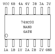
74HC00 Pinout
If you set this up on a breadboard, you will need to know the 74HC00 Pinout. I’m connecting 5v to VCC, and we also need to connect ground. Any terminal labeled A and B are particular inputs to each NAND Gate. The Y terminal for each gate is the output.
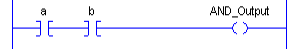
NAND Logic
At this point, look at some examples of how the NAND gate itself works. Here is a ladder logic equivalent.
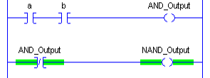
As you can see, if both A and B are true, then we would have an AND_Output. If we have the AND_Output, then we do not have the NAND_Output. However, either A or B drops out (or both), we loose the AND_Output. At this point we have a 1 on the NAND_Output.
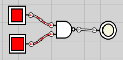
At this point, let’s look at this logic in the simulator. The color RED represents the ON state. Both inputs are true. Therefore the output is off.
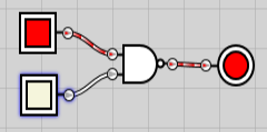
If we loose just one input, the AND part of the gate is false. Therefore, since NAND reverses the output of the AND gate, the output is ON. Remember, red is ON.
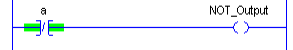
NOT Logic using only NAND Gates
The NOT gate is very simple to set up. We simply tie the inputs together. That way the inputs come from the same source. When the input is true, then both inputs are true because we tied them together. Therefore the output is LOW.
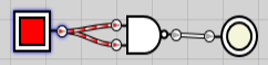
Likewise, when the input is false, the output is HIGH.
This is the equivalent of a NOT operation in Ladder Logic:
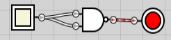
AND Logic
To create an AND gate, we simply need to add a NOT to the output of the NAND. Remember, the NAND reverses the “AND” logic. We simply need to reverse this back, and we’ll end up with an AND gate.
If both inputs are true, then our output is HIGH.
However, if we loose an input, (or both), then the output goes LOW.
In Ladder Logic, your equivalent of an AND would look similar to this:
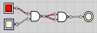
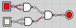
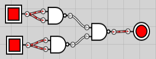
OR Logic
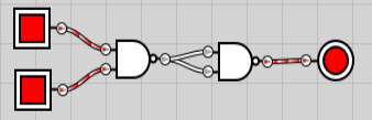
Or logic is a bit different. We’ll have to use a combination of several gates to accomplish this. You’ll have to follow this very closely to understand how the OR logic would work using only NAND gates. First, let’s take a look at the circuit.
First, we need to NOT each input. After that, we feed the result into another NAND gate. The output results in an OR operation.
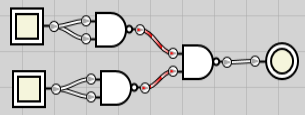
As you can see, neither input is on. Therefore the output of the first NANDs are HIGH. This means that both inputs to the second NAND is high. This results in an output that is OFF.
Let’s take a look at what happens if one of the inputs are high. As you would expect for an OR circuit, the output is HIGH. This is because the top NAND gate feeds a 0 into the send NAND gate. This results in the AND logic for the second gate being false. However, since this is a NAND circuit, it reverses this result to a logical HIGH.
The result is similar if both inputs are high. In this case, we send zeros to both the A and B input of the second NAND gate. Obviously, this results in the AND logic being false. Again, though, since this is a NAND gate, it reverses what the output would be from the AND, and the output is HIGH.
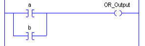
Here is the ladder logic equivalent of an OR circuit.
Check out other topics in the Beginner’s Category Page!
— Ricky Bryce