
Introduction to the 74HC595 Shift Register
The 74HC595 Shift Register allows you to control field devices based on serial input data. Although we typically use the 74HC595 Shift Register with a microcontroller, we will not do that in this post. The purpose of this post is to simply understand the operation of the shift register. Once you understand it’s operation, you can easily program a controller to make use of the shift register. I’ve put together the images using Tinkercad.
Typically, you will use the shift register to extend the number of outputs on your system. Just a few outputs on your microcontroller can control 8 outputs connected to this IC. If you need more outputs, you can easily add more shift registers.
74HC595 Shift Register Pinout
At this point, let’s take a look at the pinout of the 74HC595.
Pins 1-7 & 15
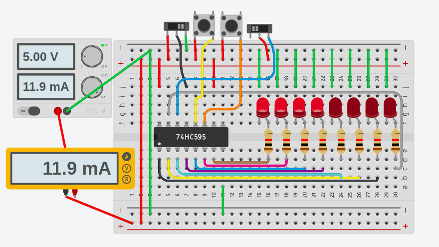
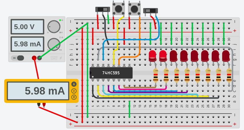
Pin 15 is for output #0, and pins 1-8 are self-explanatory. This is where you connect your 8 outputs. Do not exceed 35mA on the output pins. Likewise, do not exceed 70mA for the whole IC.
Pins 15 & 16
Pin 15 is GND. Pin 16 is your +5V (VCC). Do not exceed 70mA on either of these pins.
Pins 11, 12, & 14
DS (Pin 14) is your serial input. This pin works in conjunction with your Shift Register Clock. For example: If pin 14 stays high, and pin 12 goes from false to true 8 times, you will load eight 1’s into the shift register. When pin 11 goes high, you will then dump those eight 1’s onto the output pins, and all of the outputs will energize.
Pin 13
Be sure to hold pin 13 low to keep the outputs enabled if this is the desired state. I will give you a warning that when the chip powers up, you might not know what outputs are set to energize. In this case, be careful of unpredictable operation!
Pin 9
For this example, we’ll hold the master reclear (pin 9) high.
Circuit for the 74HC595 Shift Register
Let’s take a look at the circuit I have set up.
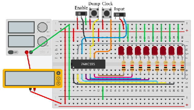
Before we begin, let’s take a look at the 4 switches/buttons above the breadboard. Enable allows the outputs to energize. This must be connected to GND for the outputs to energize. For this example, we’ll leave the outputs energized.
Our “Load” button brings a value into memory from the “Input” switch. For example: If the input switch is off, and I press the “Load” button 8 times, we load eight 0’s into memory. Likewise, if the input switch stays on, and we press the “Load” button 8 times, we load eight 1’s into memory. “Dump” then moves this data to the outputs.
The “Dump” button moves the data (8 bits) from the internal memory onto the outputs. The “DUMP” button updates the outputs.
To put it another way, if the input switch is ON, I’ll press the load button 4 times. Then I’ll shut the input switch OFF, and press the load button another 4 times. At this point, we’ll have four 1’s and four 0’s loaded into the shift register. When we press the “Dump” button, the shift register moves to the outputs. At this point, 4 outputs will be on, and 4 outputs will be off.
Let’s give this a try!
Let’s do one more example to help you understand the operation. This time, I’ll press the LOAD button twice with the INPUT switch on. Then, I’ll shut off the INPUT switch, and press the LOAD button 6 more times. Then I’ll press DUMP to update the outputs.
Summary
In short, you simply use the register clock (pin 11) to load values into memory from the input pin (14). Then you will energize pin 12 to update the outputs.
Now that you understand the operation of the shift register itself, you can write your code in the microcontroller to control the outputs. Usually, you will do this with an array of 8 bits, and a FOR loop that sets the register values to the desired state, then updates the outputs.
For more information on the shift register and examples of coding, visit arduino’s forum.
For other basic arduino information, visit the intermediate category page!
— Ricky Bryce